Building a custom RISC-V based SoC on FPGA - Part 1
Table of contents
Recently I got an idea to create my own System-on-Chip (SoC). The main purpose of this SoC is to validate a small IP in a real system: plugging it into the SoC, synthesizing it for an FPGA, writing a driver for it, and validating it in a real environment. As my motivation for doing a write-up on this project, maybe this design (and this post) will motivate someone to undertake a similar project.
My initial goal was to build an SoC similar to what is presented in this paper: The simply-V Framework: an Extensible RISC-V Reconfigurable Soft-SoC for Open Research and Fast Prototyping. I quickly found out a couple of things:
- I’m not that familiar with RISC-V ISA.
- I’m not familiar with the RISC-V ecosystem. What do I mean by that? In the paper mentioned above authors are using RISC-V Debug Module, PLIC, etc. I’m not familiar with those components, it will take me some time to become familiar with all of them.
- The main reason - I’m a bit rusty from not doing digital design for a couple of years now (my primary focus was ASIC verification) and I wanted to build as much of the design myself to ‘lube’ my digital design skills.
- I don’t know enough about embedded Linux development.
To summarize: the scope of the paper is too big for me at the moment.
My ultimate goal is to do the SoC capable of booting Linux but at the moment I’ll need a couple of simpler stepping stones before I reach that goal.
The first of many such steps is the PicoRV32 based SoC.
Choice of hardware and EDA tools
Through the years I’ve procured a couple of FPGA development boards - either at a low cost, or through my work in the Faculty of Electrical Engineering and Computing. I have the following boards at my disposal:
- Digilent Zedboard - a Zynq-7000 Development board. I bought this board while I was still a student, got it with academic discount. Paid something like ~200€ at the time for it. I’ve used this one a lot. Couple of years ago I’ve built a software defined radio (SDR) based on Analog Devices AD9364 (FMC expansion card) and ZedBoard as a carrier board.
- Avnet ULTRA96-G REV 1 - it’s an older board which got an update over the years. I’ve got this one dirt cheap, I think something like 50$ and I’ve never used it which is a complete shame. I see now there are newer versions of this board, but the old one is still good.
- Digilent Nexys Video - I’ve seen this board sitting in the University storage room, and since no-one was using it at a time I was able to borrow it, under the promise I’d develop something on it, some stuff that could be of use to the students. Well, now I have the chance to keep my promise!
I’ve settled on using the Nexys Video dev board. It’s feature rich, has enough resources to implement a decently large design, and most importantly I can use free Vivado license to synthesize the design for this board. It’s a perfect board to implement design of the size (and speed) I’m aiming at.
As for the software and simulators, initially I thought of using a complete free and open source solutions. I was thinking of using Altair DSim since it’s free for personal use, but I never got it to work with a free license. The simulator that is integrated inside a Vivado also got a boost over the years. I tried playing with it, and I’m not a big fan. The Vivado interface is clunky and I got glitches when running it on my machine - BTW I use Arch Linux.
For now I think I’ll still use commercial EDA tools. Through the university I have access to Cadence toolchain, namely to the Xcelium and JasperGold Formal tools. Since I’m not building anything commercial (everything I build and post on this blog is either going to be published in some kind of paper or it’s built for research purposes) I’ve decided to use the commercial tools for now; but I’ll most definitely switch to free/open source solutions sometime in the future.
Eventually, I want to check out Verilator and the SymbiYosys is of a particular interest to me.
Architecture
Before I start with the SoC I have to make a couple of architectural choices. The first and the most important is the type of bus I’m going to use to connect everything. Since I have a fair amount of experience with the AXI bus, I’ve decided to use it. The design I’m going to make is not a big design and I don’t need some advanced AXI features, therefore I’ve settled on an AXI4-Lite bus.
There is one more reason why I chose AXI bus - the availability of the interconnect. Initially I wanted to use Xilinx interconnect (since I’m developing for a Xilinx FPGA), but I decided to use the least amount possible of Xilinx components. There is no particular strong reason why I did it. I kinda dislike the block diagram approach and working in GUIs in general, if I use Xilinx IPs I’ll most definitely be backed into this corner at some point. To be fair, the Vivado block diagram flow is quick if you’re using Xilinx components, but if you’re not (and you’re not in the business of building your own IP suitable for Vivado use), then it becomes a big inconvenience.
If I had to name one good reason, it would be to reuse this design on an FPGAs of other vendors besides the Xilinx.
ETH Zürich provides a huge number of well designed and tapeout verified components and IPs through the PULP platform. I’ve decided to use AXI4-Lite interconnect from the PULP platform Github repository. Repository also includes a small testbench and an example on how to instantiate and use this interconnect.
About PULP Platform
The PULP Platform is an open-source, energy-efficient computing architecture developed by ETH Zürich and the University of Bologna since 2013. I won’t list all the aims of the project, you can check that out here. To me, personally, the most interesting thing is the open-source availability of the verified hardware components. And the list of components - to say the least - is impressive. Check their Github page for more details. And I also need to mention this - one of the coolest things I’ve seen in the repository is the SoC developed and taped out in an Open-Source EDA flow. I recommend readers to check this out: 34 mm2 End-to-End Open-Source 64-bit Linux-Capable RISC-V SoC in 130nm BiCMOS.
The next choice I’ve had to make is which RISC-V core to use. I had a few requirements:
- Simple to use and integrate
- Good documentation
- Support for RISC-V IMC instruction set. Why M and C? It’s quite possible that I’ll use multiplication in the software that I develop. As for the C instruction set, I don’t want to use DRAM or store my program on an SD Card. Everything should fit inside a small SRAM
- Must be either formally verified or verified in a constrained random manner against a Spike (or some other) model
- I should be able to connect the core to the AXI4-Lite interconnect via some kind of bridge, or ideally there should be a built in solution to do this
- The RISC-V core should be able to handle simple interrupts
The PicoRV32 RISC-V core satisfies all of the above. It’s a neat small RISC-V core, with good documentation and it’s very simple to integrate. Actually it’s so good, that if I was to use a simple RISC-V core in a project I was going to tapeout, this would be my choice.
As far as the rest of the components, I need a timer capability, capability to use switches, LEDs and buttons (some kind of simple GPIO), most definitely UART for communication and debugging and I also need SRAM to store the bootloader and the program being ran.
I’ve decided to build all of those components myself.
The final architecture should look something like this:

Ah and I forgot, I want everything to work on at least 100 MHz.
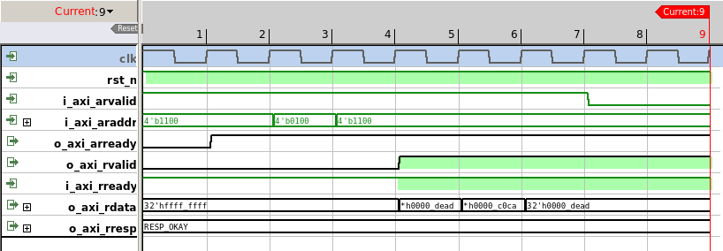
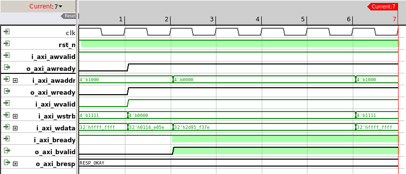
Development of AXI4-Lite SRAM module
This module is used to access static RAM via AXI4-Lite interface. This is where my programs and the bootloader will be stored. I had a couple of requirements for this module:
- Module should support back-to-back accesses on each clock cycle via AXI4-Lite interface.
- The block should be parametrizable with the SRAM bit width and the SRAM depth.
- The block should support byte access.
I won’t go into much detail how I’ve designed this. Sufficient to say, there are enough resources on
designing your own AXI4-Slave. The most useful resource I’ve found on the internet was on the ZipCPU
blog: Building the perfect AXI4 slave.
The most challenging thing I’ve had to deal with was throughput and the long backpressure path
from the slave’s AxREADY/xREADY signals. For example, the ARREADY goes from the
AXI4-Lite SRAM module to the interconnect, interconnect ARREADY goes to the PicoRV32.
This long combinatorial path resulted in not being able to close the timing for the
design. I’ve dealt with these issues of throughput and long combinatorial path by using so called Skid buffers.
I’ve used the idea from this article Building a Skid Buffer for AXI
processing.
Although the idea is fairly simple, I was actually surprised how much trouble
I’ve had implementing it. The good thing is I’ve had a formal testbench ready to verify correctness of
the AXI4-Lite protocol, and that made development of the AXI4-Lite interface a lot easier.
I encourage the reader to go through the ZipCPU blog post, the concept of Skid buffers (or register slices) is very important in digital design.
I’ve synthesized this module in Vivado and found out one interesting thing. Vivado infers Block RAM to be used for the SRAM. On my device (Artix 7 XC7A200T, Speed grade -1), BRAM should theoretically work at max frequency of ~450 MHz. But when I checked the timing report after synthesis, I found out the theoretical maximum frequency was roughly 200 MHz. The Xilinx UG473, Additional Block RAM Features in 7 Series Devices states that if you want to achieve max frequency, an additional register must be placed on the output, therefore I did that. This increases latency by 1 extra clock cycle, on top of 1 clock cycle of latency BRAM already has, but it increased the theoretical maximum frequency to roughly 350 MHz.
The AXI4-Lite protocol was verified in JasperGold FPV. The data integrity was verified by using formal scoreboarding techniques. Decent explanation of Formal Scoreboarding can be found here (note: it requires registration): Formal 101: Exhaustive Scoreboarding and Data Integrity Verification Made Easy. I would be interested to see if I could do the entire verification in SymbiYosys.
More details about the AXI4-SRAM module and the module sources are available in the following Github repository AXI4-Lite Scratchpad.
Development of AXI4-Lite Counter/Timer
For the timers, I wanted something simple. I came up with the following design:

Although this is a counter, technically it’s a timer, because it counts clock cycles. The counter integrates 32-bit prescaler that first divides the input frequency. I could’ve used less than 32-bits, but since the bus is 32-bits wide, and since I have enough resources on my dev board, I’ve settled on a 32-bit prescaler.
The counter supports setting compare (threshold) value. Each time a threshold value is reached, a threshold sticky bit is set. The threshold bit is also connected to the interrupt line, therefore when the counter reaches the threshold value an interrupt is asserted. Reading from the status register clears this threshold sticky bit.
For the AXI4-Lite interface part, I’ve used what I’ve already written and debugged for SRAM, simply cleaned it up a bit.
The design and a small driver are located in the AXI4-Lite Timer repository.
Development of AXI4-Lite UART
For the UART, I’ve initially wanted to build a 16550 compatible UART block. In the end I’ve decided not to do that. There is only one major reason: I’ll be using only the UART TX/RX lines, don’t care for the flow control. But I’ll be using some of the good features of the 16550 UART.
I decided on the following features:
- Default should be 115200 baud, 8 data bits, 1 stop bit, no parity, should work out of the box.
- I want it to support baud rates up to (and including) 921600 bits per second.
- I want it to be on-the-fly configurable.
- It shouldn’t be a burden on the CPU, it needs to use TX/RX FIFOs and it needs to support interrupts.
- I need FIFO full/empty signals in the status registers, but also I want to have configurable threshold.
First, the AXI4-Lite part. I’ve decided to reuse what I’ve had before i.e. AXI4-Lite interface with debugged handshaking, and I’ve added a couple more registers. For the FIFOs, I settled on the 16-deep FIFOs. In case a FIFO depth of 16 bytes proves to be too small, I can increase it in the future, but for now I think the size is good enough.
The weakest point of the AXI4-Lite UART is the simplicity of the testbench. I’m only verifying features in a direct test manner. In the ideal universe I would’ve done a fair bit of constrained random/metric driven verification, and should’ve built a UVM testbench, but I was too excited to see the design in action as soon as possible. Since this is not a commercial design but my own hobby project, I’ve settled on a simple testbench and validation on an FPGA board.
The design and a small driver are located in the AXI4-Lite UART.
Edit from the future
This design has been synthesized and tested on an FPGA development board. I’ve tested communication between the board and my PC with all the supported baud rates, 7 and 8 data bits, all parity values and all options of the stop bits and it works well.
If I get the chance to mentor students again in the future, the verification incompleteness of the AXI4-Lite UART could be used as a strength. I could give this to a student working on his/her bachelor thesis to learn the UVM and verify this design.
Development of a GPIO
The goal for the future is to build a fully working GPIO, but for now I’ll settle only on handling LEDs. The fully capable GPIO module will have to wait a bit. The reason why I build this ‘LED handler’ is I wanted to have some kind of built-in debugging feature once I start validating my design on the board.
In the end, I’ve settled on a single AXI4-Lite accessible register, which is connected to the LEDs. Verified in Formal, worked well. This design can be found here.
Common clock and reset (CCR) module
The purpose of the CCR module is to handle everything related to the clock and reset capability of the SoC. The CCR module is a wrapper around the vendor PLL (in this case it’s Xilinx MMCM) and the logic required to use the dedicated pushbutton on the development board as a reset button. A block diagram of the CCR module is shown in the figure below.

I want the entire design to be under reset until the PLL locks, or if the user pushes a ‘Reset’ button. Since the design is small enough, the CCR module is good as-is. If it grows too large, I have a strong suspicion I would run into clock/reset fanout issues. This is something to keep in mind for the future.
If someone wants to reuse this entire design on a different vendor FPGA, I think only this module needs to be updated.
Integration
The next thing I need to decide on is the memory map. I’ve decided to use 16-bit wide addresses (no need for 32-bits, and this reduces the size of address decoder), and decided on the following memory map:
| Address Range | Size | Peripheral | Description |
|---|---|---|---|
0x1000 - 0x1FFF |
4KB | Timer/Counter | Programmable timer with IRQ |
0x2000 - 0x2FFF |
4KB | GPIO (LEDs) | LED control interface |
0x3000 - 0x3FFF |
4KB | UART | Serial communication |
0x4000 - 0x7FFF |
16KB | SRAM | Main program memory |
0x8000 - 0x8FFF |
4KB | Bootloader ROM | UART bootloader |
The PicoRV32 is issuing 32-bit addresses, but I’m truncating this in the PicoRV32 to AXI4-Lite interconnect connection, by connecting only the 16 LSBs.
The component connection was fairly simple. I’ve used the following configuration for the AXI4-Lite interconnect:
parameter axi_pkg::xbar_cfg_t AXI_XBAR_CFG_p = '{
  NoSlvPorts:   AXI_MASTER_NBR_p,
  NoMstPorts:   AXI_SLAVE_NBR_p,
  MaxMstTrans:  2,
  MaxSlvTrans:  2,
  FallThrough:  1'b0,
  LatencyMode:  axi_pkg::CUT_ALL_AX,
  AxiAddrWidth: AXI_ADDR_BW_p,
  AxiDataWidth: AXI_DATA_BW_p,
  NoAddrRules:  AXI_SLAVE_NBR_p,
  default: '0
};
I must admit I don’t fully understand the MaxMstTrans and MaxSlvTrans parameters. My assumption
is those control the number of outstanding transactions, i.e. the MaxMstTrans controls the number
of maximum outstanding transactions coming from the Master (PicoRV32), and MaxSlvTrans probably
controls the number of outstanding transactions a slave can handle.
Since the AXI4-Lite slaves I’ve built can accept two outstanding transactions, one currently handled
and one waiting because of the skid buffer, this is the number I chose i.e. MaxSlvTrans = 2. For
the master side I’ve chosen MaxMstTrans = 2 also. But again, since PicoRV32 doesn’t pipeline
memory requests (it waits for the response before issuing the next) I think this shouldn’t matter at
all.
I’ve verified if the design works correctly for the values of MaxMstTrans and MaxSlvTrans I’ve
used and I didn’t see any issues at all.
For the LatencyMode I’ve chosen axi_pkg::CUT_ALL_AX. This is recommended latency mode in the
PULP documentation. Essentially, what this option does is it further breaks the combinatorial path of
the AxREADY/xREADY signals.
The address width is chosen to be the smallest possible, my intuition tells me this affects the width of the address decoder and therefore potential maximum frequency as a consequence.
As for PicoRV32, the documentation on their Github is excellent. I’ve created a package with all the relevant parameters used in the instantiation.
  parameter bit ENABLE_COUNTERS_p = 1;
  parameter bit ENABLE_COUNTERS64_p = 1;
  parameter bit ENABLE_REGS_16_31_p = 1;
  parameter bit ENABLE_REGS_DUALPORT_p = 1;
  parameter bit TWO_STAGE_SHIFT_p = 1;
  parameter bit BARREL_SHIFTER_p = 1;
  parameter bit TWO_CYCLE_COMPARE_p = 0;
  parameter bit TWO_CYCLE_ALU_p = 0;
  parameter bit COMPRESSED_ISA_p = 1;
  parameter bit CATCH_MISALIGN_p = 1;
  parameter bit CATCH_ILLINSN_p = 1;
  parameter bit ENABLE_PCPI_p = 0;
  parameter bit ENABLE_MUL_p = 0;
  parameter bit ENABLE_FAST_MUL_p = 1;
  parameter bit ENABLE_DIV_p = 1;
  parameter bit ENABLE_IRQ_p = 1;
  parameter bit ENABLE_IRQ_QREGS_p = 1;
  parameter bit ENABLE_IRQ_TIMER_p = 1;
  parameter bit ENABLE_TRACE_p = 0;
  parameter bit REGS_INIT_ZERO_p = 0;
  parameter bit [31:0] MASKED_IRQ_p = 32'h 0000_0000;
  parameter bit [31:0] LATCHED_IRQ_p = 32'h ffff_fff3;
  parameter bit [31:0] PROGADDR_RESET_p = 32'h 0000_8000;
  parameter bit [31:0] PROGADDR_IRQ_p = 32'h 0000_4010;
  parameter bit [31:0] STACKADDR_p = 32'h ffff_ffff;
The PicoRV32 was configured to start executing from the address 0x8000 (Bootloader). I’ve connected
Timer IRQ to the PicoRV32 IRQ[2] and UART to the PicoRV32 IRQ[3]. The reason why I didn’t use the
IRQ[0] and IRQ[1] for Timer and UART is the PicoRV32 documentation states the ecall and ebreak
instructions (exceptions) will trigger an interrupt on IRQ[0] and IRQ[1] respectively.
I’ve enabled internal counters, might come in handy if I ever have to do some performance profiling.
I’ve enabled barrel shifter, multiply and division. No need for trace.
I’ve used SRAM (Scratchpad) that I’ve developed for both the Bootloader ROM and for the SRAM. For the Bootloader, I’ve left the AXI4-Write signals unconnected.
The PicoRV32 design files include PicoRV32-to-AXI4-Lite bridge and the PicoRV32 variant that natively uses AXI4-Lite interface. I’m using the latter version, therefore I don’t need to instantiate/build any bridges, it’s easy to integrate and it works out of the box.
Top-level simulation
On the top level I wanted to check if the components are connected correctly, and whether they work after being integrated in a larger design. I want to do something simple, no major automated checks, I want to be able to confirm components work correctly after integration by checking the waveforms.
I’ve decided to do some firmware-assisted verification i.e., I’ll build a simple bootloader and
a hello_world program that will use LEDs and UART, compile them, and load them in the simulation into
the Bootloader/SRAM. There are two reasons why I want to do it this way:
- I can check the waveforms and the internals of the design in the simulation. Since I don’t have a huge multi-million gate design, simulation will be very quick and I can easily debug both the hardware and the software in the simulation.
- I’ll be able to reuse most of the firmware when I validate design on an FPGA development board.
The compilation/build process should produce the following artefacts:
- A compiled and linked binary stripped of all unnecessary debug symbols and sections. This file will be used once the design is deployed on an FPGA board. The bootloader will load this binary via the UART and execute the program.
- A .lst file that will contain the RISC-V assembly. I can use this file to verify that the compilation is successful and that generated ASM is okay,
- A file containing hexadecimal representation of a stripped binary file. This file will be loaded in the simulator.
VLSI tips
Ease of debugging and component/code reuse are some of the most important concepts in digital design and digital verification
Building RV32IMC GNU Toolchain
To be able to do that I need a GNU toolchain that can be run on a Linux x86-64 host, and I’m targeting (duh) PicoRV32 - in my case, that is RV32IMC. I’m certain there is a prebuilt GNU toolchain somewhere in the outskirts of the Interwebz, I haven’t been able to find what I need, thus I decided to build the GNU toolchain from the sources.
Since I’m using Arch, these are the steps that work for me:
# Install dependencies
sudo pacman -S base-devel git python cmake ninja gawk \
    libmpc mpfr gmp zlib expat glib2

# Clone the repository
git clone https://github.com/riscv/riscv-gnu-toolchain.git
cd riscv-gnu-toolchain

# Configure for bare-metal RV32IMC
# --prefix: installation directory
# --with-arch: target architecture
# --with-abi: application binary interface (ilp32 = int/long/pointer are 32-bit)
./configure --prefix=$HOME/riscv \
            --with-arch=rv32imc \
            --with-abi=ilp32

# Build the bare-metal toolchain (newlib-based)
# This builds: gcc, binutils, newlib, gdb
# Takes roughly one hour
sudo make -j$(nproc)

# Add the installation directory to the PATH environment variable
export PATH=$HOME/riscv/bin:$PATH

# Check version
riscv32-unknown-elf-gcc --version

# Test compile
cat > test.c << 'EOF'
int main(void) {
    volatile int x = 42;
    return x;
}
EOF

riscv32-unknown-elf-gcc -march=rv32imc -mabi=ilp32 -nostdlib -o test.elf test.c
file test.elf
# Should show: ELF 32-bit LSB executable, UCB RISC-V
Typical bare-metal compile flags that I use when building the code:
CFLAGS = -march=rv32imc \
         -mabi=ilp32 \
         -nostdlib \
         -nostartfiles \
         -ffreestanding \
         -O2 \
         -Wall
If required, the detailed instructions can be found here.
On the GNU Toolchain build steps
I’m aware the instructions on how to build GNU Toolchain for the RV32IMC target are available online, or in the 21st century you can ask LLM for the steps. The problem with the LLM/Stack Overflow/Something else instructions is I’ve not been able to successfully reproduce them without issues every time. The main reason why I’ve written down these instructions is so I don’t have to repeat the entire research/debugging process again, I just want to be able to execute and easily get the known results. To summarize, I’m mostly doing this for my own sake :-)
Generating compilation artefacts
As mentioned previously, we want to produce three targets as a result of compilation.
- A compiled and linked binary stripped of all unnecessary debug symbols and sections
- A .lst file that will contain the RISC-V assembly.
- A file containing hexadecimal representation of a stripped binary file.
To create a binary file with sections and relocation information discarded, an objcopy GNU utility
can be used:
objcopy -O binary firmware.elf firmware.bin
To view executable in an assembly form, an objdump utility can be used:
objdump -d -S firmware.elf > firmware.lst
The last thing remaining is to generate a hexadecimal representation of the binary file created with
the objcopy command. For this purpose I’ve written a small Python script:
#!/usr/bin/env python3
import sys

with open(sys.argv[1], "rb") as f:
    bindata = f.read()

# Pad to 4-byte boundary
while len(bindata) % 4 != 0:
    bindata += b'\x00'

for i in range(0, len(bindata), 4):
    w = bindata[i:i+4]
    print("%02x%02x%02x%02x" % (w[3], w[2], w[1], w[0]))
This script writes 32 bits of data in hexadecimal format into each line of the file. The output is in the little-endian format. If a binary file is not 4-byte aligned, it’s first padded with zeros to a 4-byte boundary.
Bootloader, startup.S and hello_world program for the top-level simulation
The bootloader for the simulation is very simple. It contains only one instruction - jump to the first address in the SRAM.
As for the startup files and the hello_world program itself, I won’t go into much detail. Code is
worth more than a million words, and the code is available in the rv32-shock Github repository.
Project name
I figured I have to give this project a name and I’ve settled on calling it rv32-shock. The etymology of the name is from Croatian word “Šok” (a play on the acronym SoC), which directly translates into ‘shock’ in English. Since it’s RV32 based SoC, I figured ‘rv32-shock’ is a good enough name.
startup.S is a program written in RISC-V assembly. This file is usually known as crt0.S in the
embedded world. I didn’t write this file from scratch, but instead I reused the file from PicoRV32
firmware and modified it for my own
purpose.
The file contains initialization of the registers, initialization of the stack pointer, interrupt handling routine and subfunctions that can be used to enable/disable interrupts. The interrupt handling routine performs the following:
- Saves the context,
- Executes the interrupt function,
- Restores the context,
- Continues main program execution.
The main.c does the following:
- Initializes UART
- Programs the timer to interrupt every 1 second
- Enables interrupt for the timer
Every time interrupt is triggered, a CPU will start running an interrupt routine. The interrupt
program will check if the cause of interrupt was indeed a timer. If it was, it will turn off
the currently lit LED, and it will turn on the LED next to it. After 50 seconds, CPU will execute
an ebreak instruction thus asserting a trap signal of the PicoRV32 CPU.
Handling simulation time
Waiting for 1 second in the simulation can take an eternity. On a complex, multi-million gate SoC, an actual second could take a couple of days of simulation time. Although this is not the case for this design, it’s still prudent to reduce the simulation time to be as low as possible. In the simulation, timer is not programmed to count every 1 second, but instead to ~500 clock cycles. This is good enough to validate the design and it reduces simulation time.
The startup.S and main.c form the basis for the hello_world.
Drivers for handling timer/counter and UART are copied from their own respective repositories.
The final thing needed is the linker script. At first I tried writing linker script myself. The problem with this approach is I write linker script once-a-year, and every time I have to remember how this is done all over again. There are numerous tutorials and documents online on how to do it. For example, previously I would refresh my memory by watching this YouTube series from the Fastbit Embedded Brain Academy. Since I needed a simple linker script and I wanted something done fast, this time I’ve asked the LLM for help. I’m amazed I got the linker script that worked fully on the first go, without the need for any additional debugging.
To make my life easier, I’ve created a Makefile that automates artefact generation. This Makefile
can be found in the sw/hello_world subdirectory in the rv32-shock Github repository.
Loading program into the RAM in the simulation
After building the hello_world program a .hex file is produced. This file is used to initialize
RAM in the simulation. My simulation Makefile has the possibility to take bootloader and SRAM
initialization files as parameters. If a file is provided, there is an argument in the Makefile that
is passed to the simulator, to create a define.
There are multiple ways to achieve this depending on the language used and preferences; I’ve settled
on using the $readmemh Verilog system task. The following code is a direct copy-paste from the top
level testbench.
`ifdef BOOTLOADER_INIT_FILE
initial begin
  static int fd = $fopen(`BOOTLOADER_INIT_FILE, "r");
  if (!fd) begin
    $display("Memory file %0s not found!", `BOOTLOADER_INIT_FILE);
    $fatal;
  end
  $fclose(fd);
  $readmemh(`BOOTLOADER_INIT_FILE,
    picorv32_soc_dut.axi_lite_bootloader_inst.ram_block);
end
`endif

`ifdef RAM_INIT_FILE
initial begin
  static int fd;
  fd = $fopen(`RAM_INIT_FILE, "r");
  if (!fd) begin
    $display("Memory file %0s not found!", `RAM_INIT_FILE);
    $fatal;
  end
  $fclose(fd);
  $readmemh(`RAM_INIT_FILE,
    picorv32_soc_dut.axi_lite_scratchpad_inst.ram_block);
end
`endif // RAM_INIT_FILE
Top level testbench
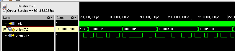
The top level testbench contains the DUT instantiation, blocks used for generating clock and reset, block of code that prints bytes received from UART and another block of code used to print the LED status. After running simulation I’m getting the following output:
LED status: 00000000
LED status: 00000001
@             86232000: RX = 0x55 ('U')
LED status: 00000010
@             97152000: RX = 0x41 ('A')
LED status: 00000100
@            108052000: RX = 0x52 ('R')
LED status: 00001000
@            118952000: RX = 0x54 ('T')

...

LED status: 00010000
LED status: 00000100
LED status: 00001000
LED status: 00010000
LED status: 00100000
LED status: 01000000
LED status: 10000000
And the waveforms display the following…
I will consider this a “good enough” design and proceed with backend work: writing constraints, synthesis, timing closure, place and route, bitstream generation, aaaand I still have to write a bootloader!
All of that (and more) will be written up in the next Part 2 of the project.
Summary
In this first part of this series I’ve covered the architectural choices, design and verification of the individual components, and integration of the PicoRV32 based SoC. The SoC includes a PicoRV32 RISC-V core connected via the PULP AXI4-Lite interconnect to an SRAM, a timer/counter, a UART, a simple LED controller, and a bootloader ROM. All components were designed with back-to-back throughput in mind, using skid buffers to break long combinatorial paths. The AXI4-Lite protocol and data integrity were verified formally in JasperGold, and the integrated design was validated in simulation using firmware-assisted verification.
In Part 2 I’ll cover the backend work: writing Vivado constraints and TCL scripts, synthesis, timing analysis and closure, place and route, and bitstream generation. I’ll also go through the development of the UART bootloader, reuse of the hello_world program, and validation on the Nexys Video FPGA board — including resource utilization numbers, achieved maximum frequency, and a video showing the whole thing in action.